Better Together: Graphene-Nanotube Hybrid Switches

Graphene has been called a wonder material, capable of performing great and unusual material acrobatics. Boron nitride nanotubes are no slackers in the materials realm either, and can be engineered for physical and biological applications. However, on their own, these materials are terrible for use in the electronics world. As a conductor, graphene lets electrons zip too fast—there’s no controlling or stopping them—while boron nitride nanotubes are so insulating that electrons are rebuffed like an overeager dog hitting the patio door.
But together, these two materials make a workable digital switch, which is the basis for controlling electrons in computers, phones, medical equipment and other electronics.
Yoke Khin Yap, a professor of physics at Michigan Technological University, has worked with a research team that created these digital switches by combining graphene and boron nitride nanotubes. The journal Scientific Reports recently published their work.
“The question is: How do you fuse these two materials together?” Yap says. The key is in maximizing their existing chemical structures and exploiting their mismatched features.
Nanoscale Tweaks
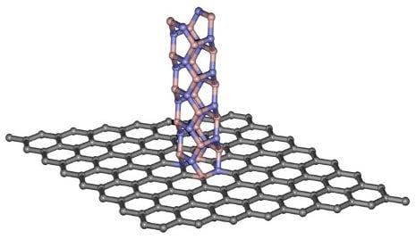
Graphene is a molecule-thick sheet of carbon atoms; the nanotubes are like straws made of boron and nitrogen. Yap and his team exfoliate graphene and modify the material’s surface with tiny pinholes. Then they can grow the nanotubes up and through the pinholes. Meshed together like this, the material looks like a flake of bark sprouting erratic, thin hairs.
“When we put these two aliens together, we create something better,” Yap says, explaining that it’s important that the materials have lopsided band gaps, or differences in how much energy it takes to excite an electron in the material. “When we put them together, you form a band gap mismatch—that creates a so-called ‘potential barrier’ that stops electrons.”

The band gap mismatch results from the materials’ structure: graphene’s flat sheet conducts electricity quickly, and the atomic structure in the nanotubes halts electric currents. This disparity creates a barrier, caused by the difference in electron movement as currents move next to and past the hair-like boron nitride nanotubes. These points of contact between the materials—called heterojunctions—are what make the digital on/off switch possible.
“Imagine the electrons are like cars driving across a smooth track,” Yap says. “They circle around and around, but then they come to a staircase and are forced to stop.”
Yap and his research team have also shown that because the materials are respectively so effective at conducting or stopping electricity, the resulting switching ratio is high. In other words, how fast the materials can turn on and off is several orders of magnitude greater than current graphene switches. In turn, this speed could eventually quicken the pace of electronics and computing.
Solving the Semiconductor Dilemma
To get to faster and smaller computers one day, Yap says this study is a continuation of past research into making transistors without semiconductors. The problem with semiconductors like silicon is that they can only get so small, and they give off a lot of heat; the use of graphene and nanotubes bypasses those problems. In addition, the graphene and boron nitride nanotubes have the same atomic arrangement pattern, or lattice matching. With their aligned atoms, the graphene-nanotube digital switches could avoid the issues of electron scattering.
“You want to control the direction of the electrons,” Yap explains, comparing the challenge to a pinball machine that traps, slows down and redirects electrons. “This is difficult in high speed environments, and the electron scattering reduces the number and speed of electrons.”
Much like an arcade enthusiast, Yap says he and his team will continue trying to find ways to outsmart or change the pinball set-up of graphene to minimize electron scattering. And one day, all their tweaks could make for faster computers—and digital pinball games—for the rest of us.
This work is supported by the U.S. Department of Energy, Office of Basic Energy Sciences, Materials Sciences and Engineering Division (Grant DE-SC0012762, PI: Y. K. Yap). The theoretical effort is supported by the US Army Research Laboratory, Weapons and Materials Directorate “Hybrid Nano and Nano-Bio Materials” Program. Part of the experimental work was conducted at the Center for Nanophase Materials Sciences (Project CNMS2012-083, PI: Y. K. Yap), and the Center for Integrated Nanotechnologies (Project U2011A1074, PI: Y. K. Yap).
Michigan Technological University is an R1 public research university founded in 1885 in Houghton, and is home to nearly 7,500 students from more than 60 countries around the world. Consistently ranked among the best universities in the country for return on investment, Michigan's flagship technological university offers more than 120 undergraduate and graduate degree programs in science and technology, engineering, computing, forestry, business, health professions, humanities, mathematics, social sciences, and the arts. The rural campus is situated just miles from Lake Superior in Michigan's Upper Peninsula, offering year-round opportunities for outdoor adventure.


Comments